UniversalPHOLED® Materials
Our patented and award-winning phosphorescent OLED (PHOLED) technology and UniversalPHOLED® materials are integral to enabling energy-efficient OLED displays and lighting. With luminous efficiencies that are up to four times higher than with conventional fluorescent OLED materials, PHOLEDs can reduce power consumption and enhance the number of AMOLED backplane choices. These important PHOLED advantages allow OLEDs to compete with LCDs and conventional light sources. In commercial use since 2003, our patented PHOLED technology and materials offer key features including:
- Record-breaking energy efficiencies
- Vibrant colors
- Long operating lifetimes
- Thermal stability for manufacturing use
- Manufacturing versatility
- Environmental-friendliness
With this rich set of features, PHOLED technology can enhance the performance of displays and lighting products – providing real power savings advantages – for longer battery operation in portable electronics and less energy consumption in larger display and lighting products.
We collaborate closely with each of our customers to custom design next-generation materials that meet their specifications for color, efficiency and lifetime. With different requirements that go across the color spectrum from deep colors to light colors for various applications, the ability to hit multiple product cycles is part of UDC’s core strength.
What is a Phosphorescent OLED (PHOLED)?
OLEDs are monolithic, solid-state devices that typically consist of a series of organic thin films sandwiched between two thin-film conductive electrodes. When electricity is applied to an OLED, charge carriers (holes and electrons) are injected from the electrodes into the organic thin films. Then, under the influence of an electrical field, these carriers are transported through the device, until they recombine forming excitons. Once formed, these excitons, or excited states, relax to a lower energy level by giving off light and/or heat.
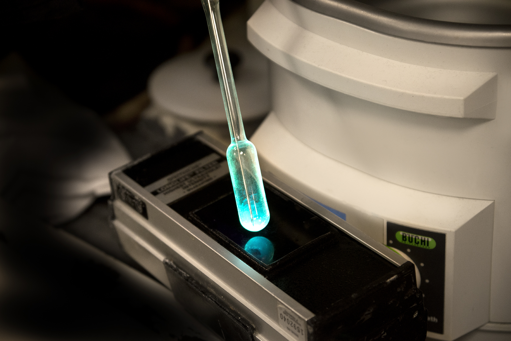
Through the use of certain phosphorescent materials, our university partners at Princeton University and the University of Southern California discovered in the late 1990s, that up to 100% of the excitonic energy could be converted into light, compare to the 25% conversion with fluorescent materials.
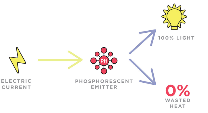
This discovery was a major breakthrough. It meant that OLEDs could be up to four times more efficient than previously thought possible. Phosphorescent technology enabled OLEDs to be more energy-efficient than LCDs (in many cases), as well as incandescent and fluorescent lighting.
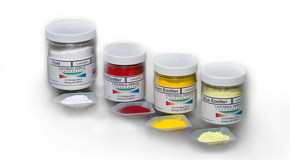
UniversalPHOLED® Materials Portfolio
Universal Display Corporation’s (UDC or the Company) proprietary product portfolio includes:
- Red, Green and Yellow Emitters for Displays;
- Red, Green, Yellow and Light Blue Emitters for Lighting; and
- Host Systems (Mixed and Single Component) for Red, Green, Yellow and Light Blue
The Company continues to advance its research work in Blue emissive materials for displays and lighting applications.
From Design to Manufacturing
UDC manages the development of new products using a staged-gatekeeper process to assess and measure success criteria in a structured way from inception to commercial production:
- Product Design. Our multi-disciplinary discovery and applications teams design and develop new high-performance PHOLED materials that strive to meet a broad spectrum of performance, quality, and EHS criteria. Moreover, the energy saving benefits of PHOLED materials help support sustainability;
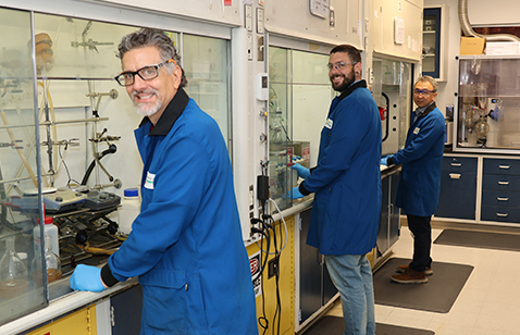
- Manufacturing Process. UDC, along with its exclusive manufacturing partner, PPG, assess and manage risks and hazards associated with the manufacture of each product, including supply chain management and the responsible sourcing of raw materials, minimizing harmful or hazardous chemicals in the Company’s products, chemical handling and exposure, waste minimization and handling (including production and e-waste), process robustness and reproducibility, and cost-effectiveness;
- Product Quality. UDC’s UniversalPHOLED materials are produced by PPG to exacting quality standards and are fully device-qualified using ISO 9001:2015 compliant quality management systems against stringent analytical and device specifications. Our products are designed, developed and manufactured to very high purity levels. Product quality and characterization are regularly confirmed through an array of analytical and toxicological testing, internal manufacturing protocols, Safety Data Sheets (SDS’s) development and regulatory compliance, e.g., EPA TSCA and Chinese, Japanese, Korean, and Taiwanese chemical import registrations, to name a few. The potential for inclusion of harmful chemicals in its products is minimal. Moreover, UDC’s existing UDC PHOLED products:
- Meet the Restriction of Hazardous Substances (RoHS) Directive 2002/95/EC requirements; and
- Do not use or contain Conflict Minerals. UDC periodically audits PPG and its raw materials suppliers to support UDC’s commitment in this area.
Design for Environment
To find additional opportunities for improvement, UDC and PPG will evaluate UDC’s products against Design for Environment (DfE) practices:
- Design for Energy Efficiency. As described above, energy efficiency is a core attribute of UDC’s products. Smartphones, televisions and other consumer electronics and lighting applications that use the Company’s UniversalPHOLED emitter products consume less energy than other comparable products.
- Design for Environmental Processing and Manufacturing. Through a detailed Environmental Staged Gatekeeper Process, the Company’s raw materials and product manufacturing are designed to minimize the generation of hazardous by-products and waste, air pollution, and energy use, as well as the risks of harm or danger to workers or the environment. In addition, UDC and PPG have implemented numerous recycling programs.
- Design for Environmental Packaging. UDC’s packaging materials used for its products sold to display and lighting panel manufacturers are environmentally friendly, as described below in UDC’s packaging policy (UDC does not sell its products directly to individual consumers).
- Design for Disposal or Reuse. The end-of-life for UDC’s products is managed very carefully by UDC and its customers. Waste streams generated from processing and manufacturing operations incorporating UDC products by UDC and its customers are recycled, where possible, or disposed in a manner to minimize the emission of chemicals into the air, ground and water.
UniversalPHOLED Product Packaging
To enhance UDC’s packaging sustainability further, our goals include:
- Continue the Company’s ‘less is more’ initiative – We believe that UDC’s current packaging system already minimizes packaging content. Our remaining primary goal is to work with key customers to continue to transition from glass to HDPE. Our target is to reduce UDC’s usage of glass bottles by 5% over the course of the year.
- Use of recyclable packaging materials – We believe that 100% of the Company’s packaging materials are recyclable. We aim to meet this target.
- Improve the recycle content – UDC will establish a baseline of recycle content in our key packaging materials and strive to increase overall recycle content.
- Re-use vs recycling – While re-use is often preferable, it is not always so. We will evaluate when and how the Company can re-use cartons, bottles and fillers, without compromising quality or performance or increasing its carbon footprint, as an aspect of UDC’s packaging waste management program.
- Packaging sustainability throughout UDC’s supply chain – In 2019, the Company started to baseline the packaging systems used by PPG and its key suppliers. In 2020, the Company will complete this assessment and establish some vendor-specific packaging targets.
UniversalP2OLED® Printable Phosphorescent OLEDs
The standard approach for manufacturing a small molecule OLED, including a PHOLED, is based on a vacuum thermal evaporation, or VTE, process. With a VTE process, the thin layers of organic material in an OLED are deposited in a high-vacuum environment. An alternate approach for manufacturing a small molecule OLED involves solution processing of the various organic materials in an OLED using techniques such as spin coating or inkjet printing onto the substrate. Solution-processing methods have been in development for over 15 years. There are a number of challenges with this method, including the ability to meet the pixel performance required for commercial specification. For several years, we worked on P2OLEDs under joint development agreements with Dupont Displays and then Seiko Epson Corporation. If solution printing process does become commercially viable, our P2OLED phosphorescent materials are available for use.